Welcome to my blog, hope you enjoy reading
RSS

Wednesday 29 February 2012

Conduction in Organic Molecule

Hey frnds, all we know that Plastics are totally insulating material, but if i say that conduction is also possible in plastics........then can u believe? But yes this is true. Don't u want to know that how this happen......here is answer of your question.
Plastic is also known as Polymer.The fundamental property that allows polymer / organic molecules to conduct electronic charge is molecular conjugation, i.e. the presence of alternating single and double bonds between covalently bound carbon atoms.Conjugation causes the delocalization of one of the four valence electrons of each carbon atom that participates in the conjugated system, and this allows the ecient transport of electronic charge along a conjugated molecule.
  Highly conjugated organic materials have the potential to work as semiconductors because of their strong π-orbital overlap. In organic solids, the carbon atom forms a tetrahedral SP3 Hybridized single bond configuration, but in double bond it has the configuration of SP2-Pz and in triple bond it has SP-Pz-Py configuration . The intra-molecular interactions between the atoms lead to a splitting of the initially degenerated 2Pz energy levels into a bonding and an anti-bonding molecular π orbital. 


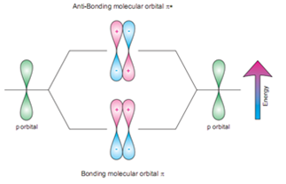
The resulting bonding orbital takes the electrons known as HOMO(Highest Occupied Molecular Orbit) while the anti-bonding orbital remains empty LUMO (Lowest Unoccupied Molecular Orbital ). HOMO is equivalent to valance band and LUMO, to conduction band. The gap between HOMO and LUMO is known as Energy band gap.


Tuesday 28 February 2012

Radio Frequency Identification Tags (RFIDs)

Hello frnds, have u heard about RFIDs.....in this post i am going to tell u about Radio Frequency Identification Tags (RFIDs) and give a brief comparison between Silicon and Organic RFIDs. Actually, RFID tag is a wireless form of automated identification technology that allows non-contact reading of data, making it effective for manufacturing, inventory, and transport environments where bar code labels are inadequate.

Advantages of organic-based RFID tags over silicon-based tags include mechanical flexibility (e.g., bendable) and direct fabrication onto large area substrates using simple printable methods. 
The attractiveness of printed organic semiconductor materials and manufacturing platforms has drawn the involvement of several companies(e.g.,3M,Siemens),start-ups(e.g.,OrganicID,ORFIDCorp.),and research institutions to develop technology for organic-based RFID tags. For example, a 64-bit inductively-coupled passive RFID tag on a plastic substrate was demonstrated, operating at 13.56MHz and with a read distance of over 10 cm.
These specifications are approaching item-level tagging requirements, paving the way for low-cost high-volume production of RFID tags, with the potential to replace barcodes.   


Monday 27 February 2012

Organic Field Effect Transistor

A Field effect transistor (FET) operates as a capacitor where one plate is the gate electrode and the other a conducting channel between two ohmic contacts-the source and drain electrodes.The density of charge carriers in  the channel is modulated by the voltage applied to the second plate of capacitor i.e. the gate electrode.Without gate source bias, very little current flows between source and drain electrode and the transistor is in the off state.Application of gate source voltage causes charging at the dielectric surface and induces charge in the semiconducting layer yielding a significant increase in conductivity in the sample, turning it to the On state. Organic field effect transistors(OFETs) are similar to the Silicon field effect transistor, except the active layer (conducting) is of organic semiconductor material. OFETs can be operated in accumulation of charges in the channel with negative gate voltages.


OTFTs are based on multilayer structure whose electrical properties are affected by device structures, characteristics of different material layers and interface between them. Depending on the position of electrodes with respect to active semiconductor and dielectric layer, there are various device structures such as Bottom Gate Bottom Contact (BGBC), Bottom Gate-Top Contact (BGTC), Top Gate-Bottom Contact (TGBC) and Top Gate-Top Contact (TGTC).


Sunday 26 February 2012

Organic Semiconductor Technology


Hi Frnds, all u r familiar with Silicon semiconductor technology, but have u listened about Organic Electronics? Today, Organic semiconductor technology has attracted considerable research interest in view of its great promise for large area, low-end, lightweight, and flexible electronics applications. Owing to their processability advantages and unique physical (i.e.,electrical, optical, thermal, and magnetic) properties, organic semiconductors can bring exciting new opportunities for broad-impact applications requiring large-area coverage, mechanical flexibility, low-temperature processing, and low cost. Thus,organic semiconductors have appeal for a broad range of devices including transistors, diodes, sensors, solar cells, and light-emitting devices. Following figure depicts a number of application domains that can benefit from the versatility of organic electronics technology.